Bally Space Invaders Pinball

Restoration

All content on this site Copyright ©2002-2006 Dave Pinx. All rights reserved.


It's here....
Well after a panic "buy it now" on ebay, i won it off a guy who sells jukeboxes and got it as a trade in (Thanx Willie) but he lives in Glasgow in Scotland and i live near Southampton on the south coast of England so....
I had to get it shipped down to here, yes the thought of shippers puts the fear into the eyes of many a collector, but luckily my good mate Malc only lives 15 minutes from Willie and so did me a big favour by going over and packing it as though it was his own, see pic above (thanx again dewd).

First impressions, well cosmetically its got to be very close to a 8 out of 10, it is extremely clean and the backbox infinity glass and artwork is unmarked. The playfield has just a little wear, but this has already been re-painted, the game itself is complete, so it was a very good buy !
I bought it as non working, which is how i like to buy all my games, as it gives me something to do, plus you save alot of money. Willie had warned me that some of the wires on the power supply were hanging out (before Willie got it) and some were label'd but apart from that it was untouched.

! All notes here are for my reference only, i will not be held responsible for any mistakes / damage done to your Pinball Machine !


Where to start...
As i already knew the power supply had wire problems, i decided to start here first and as you can see , its a beefy bugger. It consists of a large 240v ac transformer and a rectifier pcb, which has 3 connections to the pinball. J1 Playfield connector, J2 cabinet connector, J3 Backbox connector. These connectors on some pins suffer badly from getting too hot and badly burnt pins are very common.
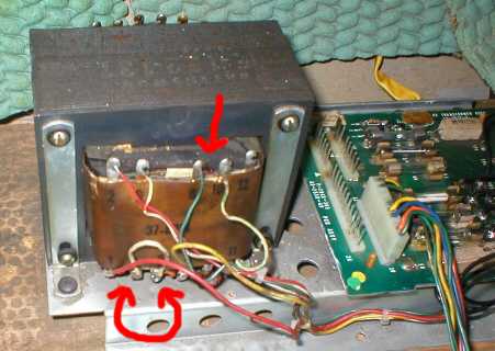
Whilst i had it on the bench, i got the manual out and checked the transformers pinouts and for UK 240v use lugs 3 and 5 should be tied with a jumper wire, but for some unknown reason this one had lugs 3 and 9 tied ! So this i changed immediately.

Burnt connections.
I then turned my attention to the large 20 pin conncetor at J3, which i could see was showing signs of burning, so i removed the loom from the table so i could work on it easier, this connector was the one which had been label'd and had 2 wires hanging out. Using a small flat bladed screwdriver i unpined all the pins from the badly burnt connector, which had burnt that much it had cracked almost in two ! (See pic)

Burnt connections cont....
I couldnt get a new 20 slot replacement connector so i went for two 10's instead and marked the connectors with paint pen showing pins 1 and 10 and pins 11 and 20, so at a glance i knew which was which. After replacing the wires in the new connectors and fitting new pins, i thought it best to check the wiring against the manual, as i couldnt be sure that who ever had label'd them had done the job properly.
I found out that this was a wise move, as 4 of the wires were in the wrong places and i mean miles out of place. So now i am expecting other pcb's within the game to be faulty, if the previous owner had been turning it on with the wires as they were, it has probably done some damage.

Power supply rectifier pcb.
Next to the transformer on the power supply is a rectifier pcb (see where to start pic), this has all the fuses for the different circuits and test points for all the voltages supplied by the power supply. It also has 2 flameproof resistors, some diodes (creating a bridge) and 2 bridge rectifiers mounted on the solder side of the pcb, these bridge rectifiers are prone to failure due to heat from the confinement of space and the fact that they are not beefy enough for the job. So i am replacing both of these before i even turn the game on ! As they do get very hot, rather than fit them back in their origional locations, i am going to fit them to a large heat sink and link them to the pcb via some jumper wires.


Bridge rectifiers.
The origional bridge rectifiers are 25 amp 200 volt, but were not beefy enough for the job, so i have replaced mine with 35 amp ones. On the pcb they are mounted underneath on the solder side, creating bad air flow, causing over heating. So i got a large heat sink and bolted both the bridge rectifiers to it after i had applied some heat sink compound to the rectifiers first (see pic)
Once i had done this, i unsolder'd the old ones from the pcb and made a note where the positive pin went. I then solder'd in some lengths of black wire to the pcb where the legs would of gone. It was then just a simple case of soldering the other end to the relative pins on each bridge rectifier, if you look at the pic you can just make out the + sign on the side (arrow'd).
After this i then tidied up the wires with a few cable ties. Next i replaced all the diodes at CR1, CR2, CR3, CR4 with new 1N4007 diodes as these suffer from heat too and as they are only pence to buy (Maplins) it paid to just replace all of them.

Rectifier pcb modifications.
The rectifier pcb has a few design faults, as some of the tracks did not have enough area for certain ground and voltage lines, which puts unnecessary strain on the connectors, causing the burning of pins etc.. To stop this problem there are a few simple modifications that can be done in the form of jumper wires (see pic). If you look at the pic, you will see that i have added a black jumper wire on the solder side of pin 5 connector J1 to pin 10 of connector J3, this adds additional area to the 7.3v ac general illumination lines.
I have then added a red jumper wire to pin 6 of connector J1 to pin 9 of connector J3, this adds additional area for the 43v dc solenoid lines. Lastly i drilled a hole to the left of connector J1 on the component side (checking that it woulndt damage anything on the solder side first!) i then solder'd one end of a black jumper wire to pins 1 and 2 of connector J1 on the solder side of the pcb, then threaded the wire through the hole i had drilled. I then scraped off some of the green solder mask in the large ground area on the component side and added a blob of solder. I then solder'd the other end of the jumper from pins 1 and 2 to this blob. This jumper adds area to the ground line for the lamp driver.

Testing the power supply.
Once these modifications had been made, it was a simple case of mounting the pcb back on the power supply and putting it back in the pinball. Now it was time to check my work and see if i had the correct volatages at the test points (TP's).
To do this i connected J2 connector (arrow'd) only, as this is the connector that supplys the volts AC to the transformer. By leaving connectors J1 and J3 disconnected, if the voltages are wrong it cant cause any damage to the pcb's in the backbox.
I now turned on the game and put the black lead of my multimeter on resistor R1's lead closest to the connectors (ground) and then in turn put my red lead on each of the test points and checked the readings.
They should approximately read this:

TP1= 8.2 vdc
TP2 =195 vdc (could be as low as 150v)
TP3 =13.5 vdc
TP4= 7.5 vac *note this is ac, change setting on multimeter
TP5 = 47 vdc

Transformer problems.
Measuring all the test points (TP's) showed that all my voltages were correct except for one, the 195 vdc line, which was only showing 45 vdc and would then work its way down towards zero !
So i knew i had a bad short somewhere. As i had rebuilt the rectifier pcb and performed some jumper mods i checked these first, but everything was ok, so i decided to take another look at the transformer itself.
As i had found earlier that the jumper wire between lugs 3 and 5 were in the wrong place for UK 240 vac i checked all the other lugs and found that lug 10 was bent over touching lug 8 and was causing the short !
So i bent pin 10 back up straight with needle nosed pliers (top arrow in pic).
I then re-meter'd all the TP's again, and voila all voltages were present and correct.

*Note bottom arrows in pic shows lugs 3 and 5 tied for UK 240V use.

Backbox Game pcb's.
Now that i was happy with the voltages, i connected J1 and J3 to the power supply and turned the game on. This gave me playfield lights and some of the backbox lights but no game. So i opened the backbox and looked at the green LED on the MPU pcb. Most Bally pinball machines from 1979 to 1985 have an on board diagnostic feature. This is where the CPU processor runs seven groups of tests looking for failed components.
With the backbox open so you can see the LED on the MPU pcb, power the game on, you should get a quick flicker flash and then seven steady pulse flashes. If you do not get all these flashes, there is something wrong with the MPU pcb and there was with mine, as i was only getting flicker flash and then two flashes.
Luckily as i had the flicker flash, this told me that the CPU was working and that the initial boot sequence was ok. As i had flash 1 it meant that all my ROM's were ok and finally as i had Flash 2 it meant that my U7 RAM was ok too.
As i had no 3rd flash this meant that my 5101 CMOS RAM or its socket was faulty.

Mpu pcb testing.
As any Williams Defender owner knows, 5101 CMOS RAM works in conjunction with the on board battery for the memory back up of highest scores and book keeping for the engineer.This is the most common fault on faulty Defender pcb's.
These CMOS RAM chips are quite hard to find now as they are no longer made and due to the age of any chips still in existance today, there is no guarantee that a new one will work when you get one. I managed to find a reliable source and bought 3 of them, one for the pinball, one as a spare for the pinball and one as a spare for me Defender :)
Expect to pay anywhere between £4.50 to £10.00 for one of these chips and just hope its a good source.
Once this had arrived i took the MPU pcb out and removed the old 5101 i then bleeped all the pins on the socket with my multimeter on continuity to make sure it was good, once i was happy with this i inserted the new chip. Rather than just install it back in the pinball and try it, i tested it on the bench using the power supply from my test rig. To do this i just hooked up :
ground,12V+,5V+ (dc voltages) using alligator clip jump wires.
This then gave me 6 Flashes but not 7 as the 7th flash is the cpu testing the 43 vdc for the solenoids.

MPU pcb ground modification.
This pcb also needs to have a jumper mod done to relieve burning to pins 18 and 19 on connection J4 as this is the only place the the MPU pcb gets its ground from the power supply. So i added a small black jumper from pins 18 and 19 on the solder side of the pcb to the large ground trace to the right of them. (see pic).

MPU pcb Battery removal.
These are nothing but trouble, as they leak corrosive acid on the pcb, which in some cases can spread quite badly, i have been lucky as the one on my machine had only leaked a little bit and not reached any components surrounding it.
I am going to replace this with a 1 Farad memory capacitor, as you can fit it and never worry about leakage again.

Click here for Page two

Or click here for Home